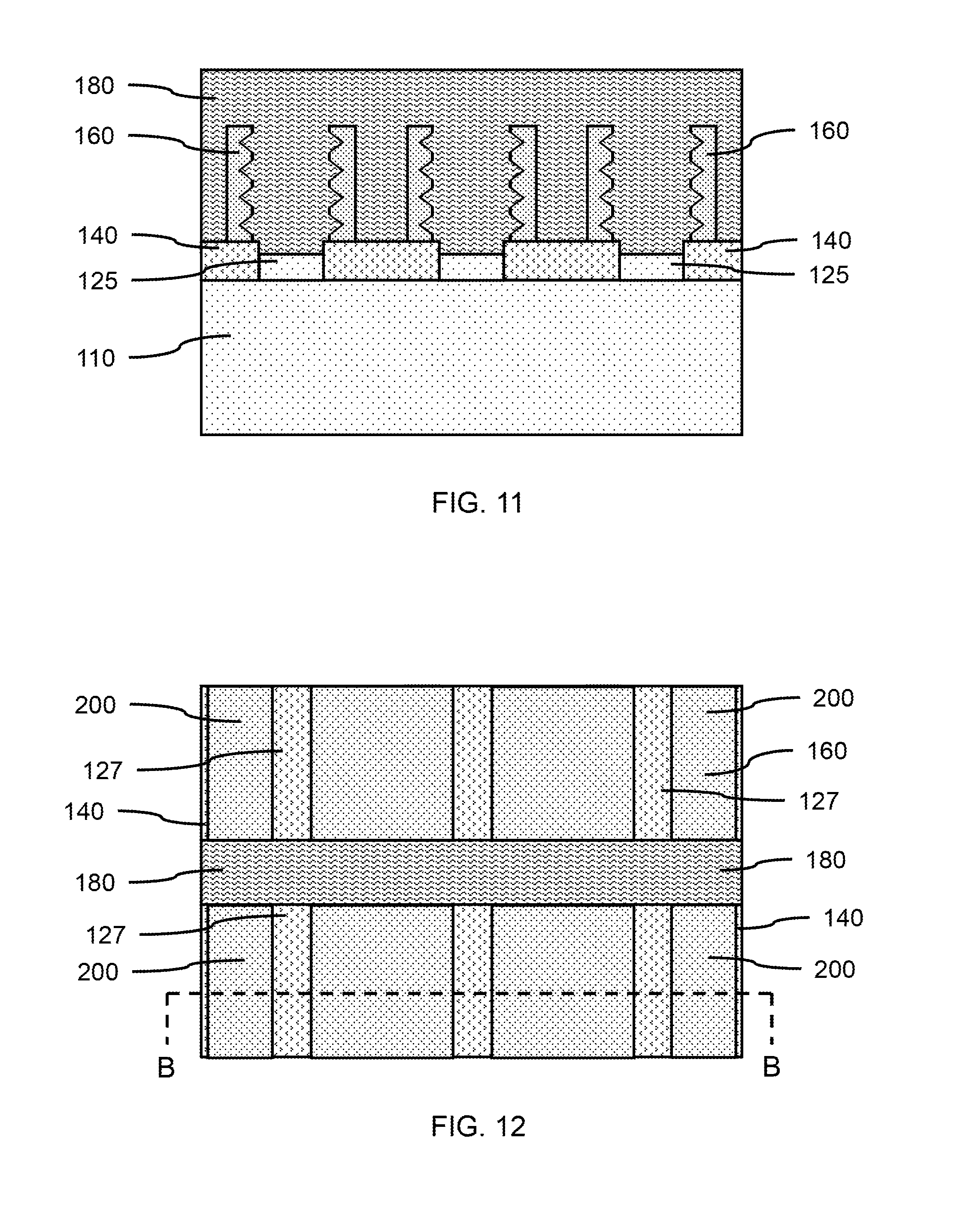
Mandrel Semiconductor . These residuals that encircle the hard mask shapes are called spacers. Sadp uses a deposition and etch step process to create spacers surrounding a patterned shape (figure 1). This deposited layer is then etched to leave residuals on each side of the hard mask. The mandrels are the patterns that define where the sidewall spacers are subsequently situated. (a) saqp process with two hard mandrels (ref. The mandrel mask is used to pattern a hard mask layer that is then covered with a new deposited layer. Both spacers can be sio 2 prepared. As you can see, there are two masking steps—the first mask is called the mandrel mask, and the second is called the block mask.
from uspto.report
The mandrels are the patterns that define where the sidewall spacers are subsequently situated. Both spacers can be sio 2 prepared. This deposited layer is then etched to leave residuals on each side of the hard mask. The mandrel mask is used to pattern a hard mask layer that is then covered with a new deposited layer. As you can see, there are two masking steps—the first mask is called the mandrel mask, and the second is called the block mask. (a) saqp process with two hard mandrels (ref. These residuals that encircle the hard mask shapes are called spacers. Sadp uses a deposition and etch step process to create spacers surrounding a patterned shape (figure 1).
Smoothing Surface Roughness Of Iiiv Semiconductor Fins Formed From
Mandrel Semiconductor The mandrel mask is used to pattern a hard mask layer that is then covered with a new deposited layer. Both spacers can be sio 2 prepared. These residuals that encircle the hard mask shapes are called spacers. Sadp uses a deposition and etch step process to create spacers surrounding a patterned shape (figure 1). As you can see, there are two masking steps—the first mask is called the mandrel mask, and the second is called the block mask. The mandrel mask is used to pattern a hard mask layer that is then covered with a new deposited layer. The mandrels are the patterns that define where the sidewall spacers are subsequently situated. (a) saqp process with two hard mandrels (ref. This deposited layer is then etched to leave residuals on each side of the hard mask.
From dgdx-elec.com
OEM factory directly highspeed steel winding mandrel end set for Mandrel Semiconductor Sadp uses a deposition and etch step process to create spacers surrounding a patterned shape (figure 1). Both spacers can be sio 2 prepared. This deposited layer is then etched to leave residuals on each side of the hard mask. These residuals that encircle the hard mask shapes are called spacers. (a) saqp process with two hard mandrels (ref. As. Mandrel Semiconductor.
From appliedplastics.com
0.0440″ X 73″ Uncoated Stainless Steel Mandre Mandrel Semiconductor (a) saqp process with two hard mandrels (ref. The mandrel mask is used to pattern a hard mask layer that is then covered with a new deposited layer. The mandrels are the patterns that define where the sidewall spacers are subsequently situated. As you can see, there are two masking steps—the first mask is called the mandrel mask, and the. Mandrel Semiconductor.
From www.researchgate.net
Crystal encapsulation steps (1) preform a polyester shrink tube, (2 Mandrel Semiconductor These residuals that encircle the hard mask shapes are called spacers. Both spacers can be sio 2 prepared. As you can see, there are two masking steps—the first mask is called the mandrel mask, and the second is called the block mask. (a) saqp process with two hard mandrels (ref. The mandrels are the patterns that define where the sidewall. Mandrel Semiconductor.
From www.hainbuchamerica.com
Micro mandrel, for clamping the smallest diameters [5,6 15 mm Mandrel Semiconductor The mandrels are the patterns that define where the sidewall spacers are subsequently situated. Sadp uses a deposition and etch step process to create spacers surrounding a patterned shape (figure 1). This deposited layer is then etched to leave residuals on each side of the hard mask. The mandrel mask is used to pattern a hard mask layer that is. Mandrel Semiconductor.
From semiengineering.com
Semiconductor Engineering SelfAligned Double Patterning—Part Deux Mandrel Semiconductor The mandrels are the patterns that define where the sidewall spacers are subsequently situated. (a) saqp process with two hard mandrels (ref. As you can see, there are two masking steps—the first mask is called the mandrel mask, and the second is called the block mask. Sadp uses a deposition and etch step process to create spacers surrounding a patterned. Mandrel Semiconductor.
From uspto.report
Smoothing Surface Roughness Of Iiiv Semiconductor Fins Formed From Mandrel Semiconductor Sadp uses a deposition and etch step process to create spacers surrounding a patterned shape (figure 1). The mandrel mask is used to pattern a hard mask layer that is then covered with a new deposited layer. The mandrels are the patterns that define where the sidewall spacers are subsequently situated. (a) saqp process with two hard mandrels (ref. This. Mandrel Semiconductor.
From dgdx-elec.com
OEM factory directly highspeed steel winding mandrel end set for Mandrel Semiconductor The mandrel mask is used to pattern a hard mask layer that is then covered with a new deposited layer. These residuals that encircle the hard mask shapes are called spacers. Both spacers can be sio 2 prepared. This deposited layer is then etched to leave residuals on each side of the hard mask. (a) saqp process with two hard. Mandrel Semiconductor.
From www.spie.org
Highly selective dryplasmafree chemical etch technique for advanced Mandrel Semiconductor As you can see, there are two masking steps—the first mask is called the mandrel mask, and the second is called the block mask. (a) saqp process with two hard mandrels (ref. The mandrels are the patterns that define where the sidewall spacers are subsequently situated. These residuals that encircle the hard mask shapes are called spacers. This deposited layer. Mandrel Semiconductor.
From uspto.report
Smoothing Surface Roughness Of Iiiv Semiconductor Fins Formed From Mandrel Semiconductor (a) saqp process with two hard mandrels (ref. These residuals that encircle the hard mask shapes are called spacers. The mandrel mask is used to pattern a hard mask layer that is then covered with a new deposited layer. The mandrels are the patterns that define where the sidewall spacers are subsequently situated. This deposited layer is then etched to. Mandrel Semiconductor.
From uspto.report
Smoothing Surface Roughness Of Iiiv Semiconductor Fins Formed From Mandrel Semiconductor Sadp uses a deposition and etch step process to create spacers surrounding a patterned shape (figure 1). The mandrels are the patterns that define where the sidewall spacers are subsequently situated. This deposited layer is then etched to leave residuals on each side of the hard mask. (a) saqp process with two hard mandrels (ref. As you can see, there. Mandrel Semiconductor.
From uspto.report
Method for mandrel and spacer patterning Patent Grant Lin , et al. A Mandrel Semiconductor Both spacers can be sio 2 prepared. These residuals that encircle the hard mask shapes are called spacers. (a) saqp process with two hard mandrels (ref. The mandrel mask is used to pattern a hard mask layer that is then covered with a new deposited layer. This deposited layer is then etched to leave residuals on each side of the. Mandrel Semiconductor.
From semiengineering.com
What Drives SADP BEOL Variability? Mandrel Semiconductor Both spacers can be sio 2 prepared. (a) saqp process with two hard mandrels (ref. These residuals that encircle the hard mask shapes are called spacers. The mandrel mask is used to pattern a hard mask layer that is then covered with a new deposited layer. This deposited layer is then etched to leave residuals on each side of the. Mandrel Semiconductor.
From www.sandparts.com
Mandrel 2.760 BBC Mandrel Semiconductor The mandrels are the patterns that define where the sidewall spacers are subsequently situated. This deposited layer is then etched to leave residuals on each side of the hard mask. The mandrel mask is used to pattern a hard mask layer that is then covered with a new deposited layer. Both spacers can be sio 2 prepared. These residuals that. Mandrel Semiconductor.
From www.hainbuch.com
Special mandrels optimized production process Hainbuch GmbH Mandrel Semiconductor These residuals that encircle the hard mask shapes are called spacers. Both spacers can be sio 2 prepared. The mandrels are the patterns that define where the sidewall spacers are subsequently situated. This deposited layer is then etched to leave residuals on each side of the hard mask. As you can see, there are two masking steps—the first mask is. Mandrel Semiconductor.
From www.sandparts.com
Mandrel 2.760 BBC PTR050713 Mandrel Semiconductor As you can see, there are two masking steps—the first mask is called the mandrel mask, and the second is called the block mask. Both spacers can be sio 2 prepared. (a) saqp process with two hard mandrels (ref. This deposited layer is then etched to leave residuals on each side of the hard mask. Sadp uses a deposition and. Mandrel Semiconductor.
From blogs.sw.siemens.com
SelfAligned Double Patterning, Part Deux Design with Calibre Mandrel Semiconductor Both spacers can be sio 2 prepared. The mandrels are the patterns that define where the sidewall spacers are subsequently situated. (a) saqp process with two hard mandrels (ref. Sadp uses a deposition and etch step process to create spacers surrounding a patterned shape (figure 1). This deposited layer is then etched to leave residuals on each side of the. Mandrel Semiconductor.
From ecatalog.system3r.com
4 results for 3Refix Mandrel Semiconductor (a) saqp process with two hard mandrels (ref. The mandrels are the patterns that define where the sidewall spacers are subsequently situated. These residuals that encircle the hard mask shapes are called spacers. The mandrel mask is used to pattern a hard mask layer that is then covered with a new deposited layer. Both spacers can be sio 2 prepared.. Mandrel Semiconductor.
From dgdx-elec.com
OEM factory directly highspeed steel winding mandrel end set for Mandrel Semiconductor This deposited layer is then etched to leave residuals on each side of the hard mask. Sadp uses a deposition and etch step process to create spacers surrounding a patterned shape (figure 1). These residuals that encircle the hard mask shapes are called spacers. (a) saqp process with two hard mandrels (ref. Both spacers can be sio 2 prepared. The. Mandrel Semiconductor.